Sputtering Equipment Market Size to Hit USD 4.19 Billion by 2035 | Research by SNS Insider

The U.S. Sputtering Equipment Market is forecast to be worth approximately USD 0.56 billion in 2025 and will grow to reach an estimated value of USD 0.94 billion by 2035, at a CAGR of 5.31%. Meanwhile, The Europe Sputtering Equipment Market is estimated to be USD 0.55 Billion in 2025 and is projected to reach USD 0.91 Billion by 2035, rising at a CAGR of 5.12% during 2026–2035. Driven by Rising Semiconductor Fabrication and Thin-Film Deposition Demand.
Austin, June 19, 2026 (GLOBE NEWSWIRE) — Sputtering Equipment Market Size & Growth Insights:
According to the SNS Insider, “The global Sputtering Equipment Market Size was valued at USD 2.41 Billion in 2025 and is projected to reach USD 4.19 Billion by 2035, expanding at a CAGR of 5.83% during 2026–2035.”
Rising Semiconductor and Electronics Manufacturing Accelerates Market Growth
Rising demand for high-performance semiconductors, flat panel displays, photovoltaic solar cells, and consumer electronics products is expected to fuel the use of sputtering equipment globally. Advanced techniques like magnetron sputtering and PVD are being used by semiconductor fabs and electronics producers for thin film deposition applications requiring utmost precision. Over 60% of semiconductor firms and electronics fabs employed sputtering equipment for the thin film deposition process in 2025. Increasing expenditure on semiconductor fabrication facilities, along with technological progress in the area of thin film deposition, is helping boost the growth of the market.
Get a Sample Report of Sputtering Equipment Market Forecast @ https://www.snsinsider.com/sample-request/9931
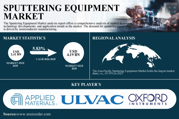
Leading Market Players with their Product Listed in this Report are:
- Applied Materials, Inc.
- Lam Research Corporation
- ULVAC, Inc.
- Tokyo Electron Limited
- Oxford Instruments plc
- Veeco Instruments Inc.
- Denton Vacuum LLC
- Kurt J. Lesker Company
- AJA International, Inc.
- Buhler Group
- Singulus Technologies AG
- CVD Equipment Corporation
- SPTS Technologies Ltd. (KLA Corporation)
- Advanced Energy Industries, Inc.
- Plasma-Therm LLC
- Canon Anelva Corporation
- Hitachi High-Tech Corporation
- Showa Shinku Co., Ltd.
- ULVAC Cryogenics Inc.
- Trion Technology Inc.
Sputtering Equipment Market Report Scope:
| Report Attributes | Details |
| Market Size in 2025E | USD 2.41 Billion |
| Market Size by 2035 | USD 4.19 Billion |
| CAGR | CAGR of 5.83% From 2026 to 2035 |
| Report Scope & Coverage | Market Size, Segments Analysis, Competitive Landscape, Regional Analysis, DROC & SWOT Analysis, Forecast Outlook |
| Key Segmentation | • By Product Type (RF Sputtering Equipment, DC Sputtering Equipment, Magnetron Sputtering Equipment, Reactive Sputtering Equipment, Others) • By Target Material (Metal Targets, Compound Targets, Ceramic Targets, Alloy Targets, Others) • By Technology (Physical Vapor Deposition (PVD), Magnetron Sputtering, Ion Beam Sputtering, Plasma-Based Sputtering, Others) • By End-User (Semiconductor Manufacturers, Electronics & Semiconductor Foundries, Solar Energy Companies, Research & Academic Institutes, Others) • By Application (Semiconductors & Electronics, Solar Photovoltaics, Displays, Optical Coatings, Others) |
Purchase Single User PDF of Sputtering Equipment Market Report (20% Discount) @ https://www.snsinsider.com/checkout/9931
Key Segmentation Analysis:
By Product Type
Magnetron Sputtering Equipment held the largest revenue share of 42.25% in the year 2025 as a result of its excellent deposition rate, plasma stability, and extensive application in semiconductor manufacturing, displays, and electronics production. The fastest-growing segment in the industry is projected to be Reactive Sputtering Equipment, with a CAGR of 7.42%. This growth will be driven by rising demand for Reactive Sputtering Equipment due to its ability to deposit compound thin films.
By Target Material
The Metal Targets segment had the highest market share of 47.21% during the forecast year 2025, attributed to its wide application in semiconductor fabrication processes, electronics industry, and metal coating process in industries. The Compound Targets segment is expected to witness the highest growth with a CAGR of 7.41% from 2026 to 2035 due to increasing demand for compound semiconductors and other electronic devices.
By Technology
During 2025, Magnetron Sputtering was the technology with the highest market share at 49.25%, owing to its efficient deposition process and applicability in large-scale production for semiconductors and displays. Plasma-Based Sputtering will be the most rapidly growing technology in terms of CAGR at 8.86% from 2026 to 2035, due to improvements in plasma control technologies and expanding usage in research and advanced electronics applications globally.
By End-User
Semiconductor Manufacturers emerged as the front-runner with a market share of 37.12%, fueled by rising demand for innovative wafer manufacturing and semiconductor chip manufacturing. Solar Energy Companies will see the highest growth rate at a CAGR of 9.05%, due to rising investments being made towards the manufacturing of thin film photovoltaics.
By Application
Semiconductors & Electronics accounted for 45.25% of the market share due to the widespread use of sputtering equipment in integrated circuits, microchips, and electronic products. The Solar Photovoltaics segment is expected to witness the highest growth with a CAGR of 8.06%, supported by global investments in renewable energy and solar industry growth until 2035.
Regional Analysis
Asia-Pacific was the highest revenue contributor, holding a market share of 45.35%, in 2025, followed by which it will continue to be the fastest growing regional market with a CAGR of 6.62% from 2026 to 2035. The growth is driven by huge investment in semiconductors, fast-paced electronics manufacturing, growth in solar PV industry, and government-led initiatives toward semiconductor self-reliance.
North America still manages to have a strong hold in the market because of its state-of-the-art semiconductor wafer fabrication facilities and the availability of high-end research and development resources as well as investments in local semiconductor production. The increasing use of modern sputter equipment for semiconductor fabrication and military electronics contributes to regional growth.
Do you have any specific queries or need any customized research on Sputtering Equipment Market? Submit your inquiry here @ https://www.snsinsider.com/enquiry/9931
Recent Developments
- September 2025, Applied Materials expanded its advanced PVD portfolio with next-generation deposition platforms designed for sub-5nm semiconductor nodes, improving film precision, process control, and manufacturing throughput.
- August 2025, Lam Research introduced upgraded plasma deposition platforms featuring enhanced uniformity control and improved process stability to support advanced-node semiconductor fabrication.
Exclusive Sections of the Sputtering Equipment Market Report (The USPs):
- SEMICONDUCTOR FAB EXPANSION ANALYSIS – evaluates global semiconductor fabrication investments and their impact on sputtering equipment demand.
- THIN-FILM DEPOSITION TECHNOLOGY BENCHMARKING – compares magnetron, reactive, RF, and plasma-based sputtering technologies across applications.
- TARGET MATERIAL UTILIZATION ASSESSMENT – provides insights into adoption trends for metal and compound targets across industries.
- ADVANCED NODE MANUFACTURING OUTLOOK – analyzes sputtering requirements for next-generation semiconductor process technologies.
- SOLAR PHOTOVOLTAIC MANUFACTURING OPPORTUNITIES – identifies growth potential arising from expanding thin-film solar cell production.
- REGIONAL INVESTMENT AND SUPPLY CHAIN ANALYSIS – evaluates semiconductor, electronics, and renewable energy infrastructure developments shaping market growth.
About Us:
SNS Insider is one of the leading market research and consulting agencies that dominates the market research industry globally. Our company’s aim is to give clients the knowledge they require in order to function in changing circumstances. In order to give you current, accurate market data, consumer insights, and opinions so that you can make decisions with confidence, we employ a variety of techniques, including surveys, video talks, and focus groups around the world.
Read Other Trending Reports:
Semiconductor Foundry Market Size, Share & Trends, 2026
Semiconductor Etch Equipment Market Size, Share & Trends, 2026
Flux for Semiconductor Market Size, Share & Trends, 2026
Semiconductor Packaging Materials Market Size, Share & Trends, 2026
Semiconductor Photoresist Stripping Market Size, Share & Trends, 2026
Semiconductor Gas Abatement Systems Market Size, Share & Trends, 2026
CONTACT: Contact Us: Rohan Jadhav - Principal Consultant Phone: +1-315-961-9094 (US)
 Disclaimer: The above press release comes to you under an arrangement with GlobeNewswire. IndiaEveningPost.com takes no editorial responsibility for the same.